
How Cypris Empowers R&D Teams


Keep Reading
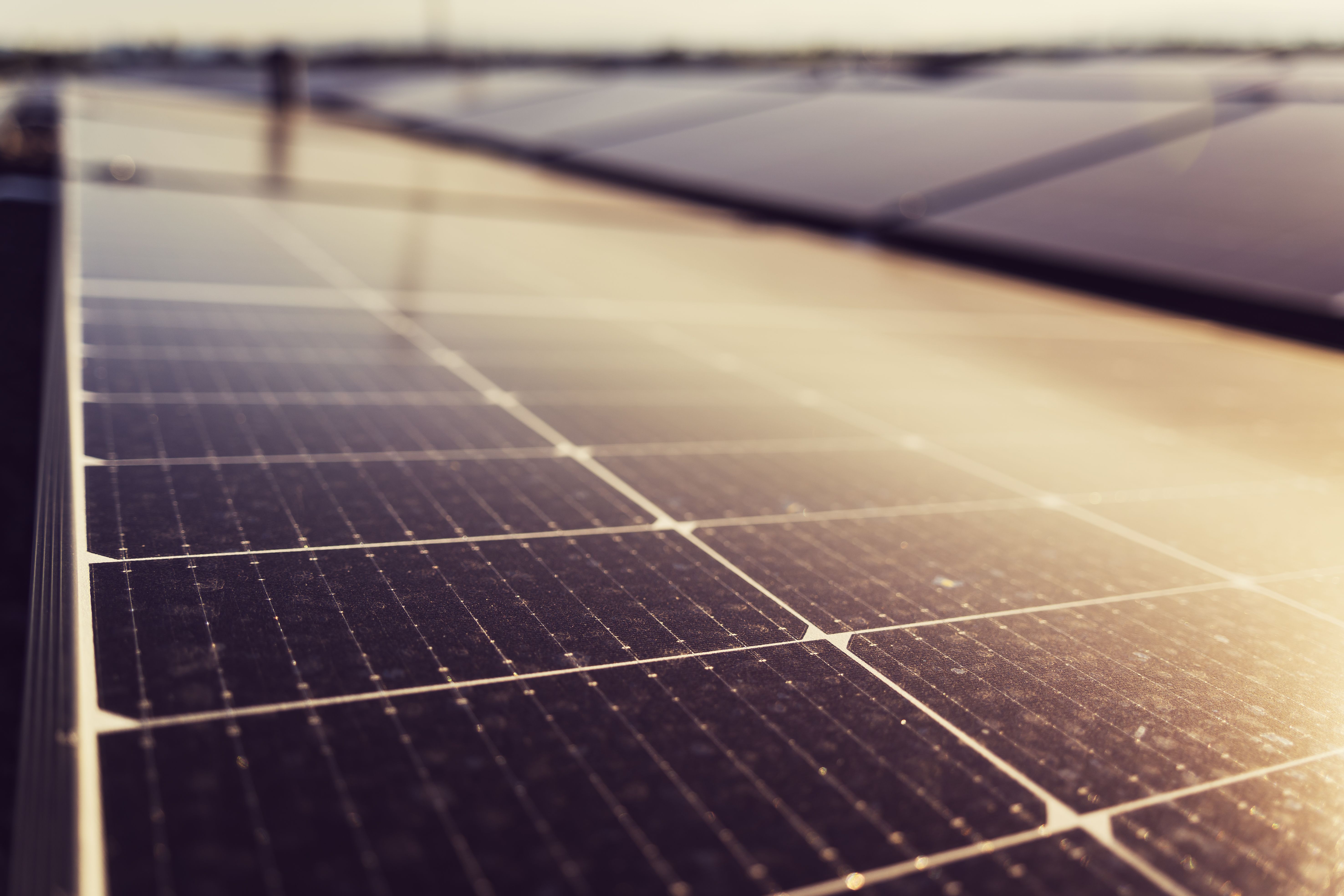
Perovskite-silicon tandem solar cells have become the clearest path to a real jump in solar-panel efficiency in decades, and their patent landscape is distinctive because the underlying physics gives every developer the same target while leaving wide latitude in how to reach it. A single-junction silicon cell is capped by a physical ceiling that combines the Shockley-Queisser detailed-balance limit with Auger recombination losses; a Fraunhofer ISE analysis that combines both effects puts the accurate theoretical efficiency limit for a silicon-based monolithic tandem at 43.2 percent¹. The path to that ceiling runs through several distinct patenting layers. Interface passivation is currently the dominant lever on record efficiency: mixed self-assembled monolayer (SAM) contacts first enabled a certified 28.3 percent tandem², further interface-passivation work pushed a certified cell to 31.25 percent³, and subsequent bilayer SAM strategies have continued to close the non-radiative recombination gap⁴. A separate, equally central problem is depositing perovskite uniformly onto the pyramid-textured surface of industrial silicon wafers — the texture that gives production-grade silicon its light-trapping advantage also makes uniform, defect-free perovskite deposition difficult, typically causing localized electrical leakage at the pyramid peaks. Proposed fixes include selective passivation of the pyramid tips specifically (32.9 percent reported)⁵, "iceberg-like" pyramid engineering compatible with industrial texturing (33 percent)⁶, and advanced light-management approaches for textured interfaces more broadly⁷. Because record efficiency and manufacturable durability are driven by different, not always overlapping, sets of techniques, freedom-to-operate and white space analysis must span composition, interface, and texture-compatible process together.
The field has moved from a laboratory curiosity to early commercial shipment within the past two years, even as the record-chasing and the product-shipping efforts remain distinct. The current widely cited two-terminal cell efficiency record is 34.85 percent, announced by LONGi and stated by the company to be NREL-certified — a figure that should be read as certified-per-developer disclosure at cell area, since the independent certification certificate itself was not directly available in this research pass, and it is not (as of this writing) also a peer-reviewed published result⁸. This record is categorically distinct from module-level performance: Oxford PV and Fraunhofer ISE reported a full-size commercial-format module at 25 percent efficiency, a genuinely different, lower, and non-comparable figure because module-area results inherently lag cell-area records⁹. Preserving this cell-versus-module distinction, and the related single-junction-perovskite-versus-tandem distinction, matters throughout any reading of the field's efficiency claims. Commercial shipment and pilot-line status is confirmed via primary company disclosure for Oxford PV⁹; comparable primary shipment-volume disclosures for other major developers were not located in this pass and should be treated as unconfirmed pending each company's own investor-relations or regulatory filing. Because applications publish about eighteen months after filing, the most recent passivation and encapsulation filings are under-represented, so the current frontier is more active than granted-patent counts suggest.
The strategic picture turns on which side of the record-versus-durability divide an owner is defending. Efficiency-record IP, concentrated in interface-passivation chemistry, is advancing quickly through a small number of well-resourced developers and research groups, and durability improvements are increasingly bundled with efficiency claims rather than reported separately in the most recent literature. The more open, commercially decisive ground remains the manufacturing and durability layer: deposition techniques compatible with textured industrial silicon at scale, and encapsulation and barrier-layer chemistry that closes the stability gap with silicon's multi-decade outdoor lifetime. Reading the landscape by layer, technique, and owner, and tracking both the patents and the underlying materials-science research, is what separates a workable manufacturing position from a blocked one.
Where the perovskite-silicon tandem white space is
Textured-silicon-compatible deposition. Depositing a uniform, leakage-free perovskite layer onto the pyramid-textured surface of industrial silicon wafers, rather than the flat substrates used for the highest record cells, is the central manufacturing barrier standing between lab records and mass production, with several distinct proposed solutions still competing⁵,⁶,⁷.
Encapsulation and durability chemistry bundled with efficiency. The most recent passivation literature increasingly targets stability and efficiency together rather than treating them as separate problems, which is itself a signal of where the field is converging.
Verified, primary-sourced commercial shipment data. Commercial shipment status is confirmed for Oxford PV via primary disclosure; comparable confirmation for other major developers remains outstanding, making rigorously verified shipment and production-volume claims a genuine differentiator.
Module-scale (not just cell-scale) efficiency. Because record efficiency is consistently reported at small cell area while commercial products are judged at full module scale, IP and technique that closes this cell-to-module gap is disproportionately valuable relative to further small-area record chasing.
Flexible and building-integrated form factors. Solution-processable, flexible tandem cells for curved surfaces, windows, and other building-integrated applications exploit perovskite's inherent advantages rather than competing directly with rigid silicon, and remain a less-crowded adjacent frontier.
How AI-powered landscape and white space analysis helps
Resolving a landscape that spans perovskite composition, interface chemistry, texture-compatible deposition, and encapsulation — where record-setting efficiency claims are announced by multiple developers within the same quarter, and where cell-area, module-area, certified, and company-announced figures are easily conflated — requires more than keyword search. AI-powered analysis addresses this with semantic search that clusters activity by layer and technique across varied terminology, attribution that normalizes solar-manufacturer, materials-supplier, and research-institution filers to canonical entities, and continuous monitoring that keeps pace with a field where the efficiency record itself changes multiple times a year. Because photovoltaics advances appear in materials-science literature before they are patented, reading both patents and literature gives the earliest signal of which technique is actually closing the gap between record cell and bankable product.
The competitive landscape by the numbers
The perovskite/tandem solar-cell patent family set totals roughly 12,575 documents, though this figure includes broader "tandem solar cell" and general photovoltaics art and therefore overstates perovskite-silicon-specific filings on its own (Cypris corpus, indicative; 2025–26 partial). Geography is led by China (approximately 1,994 families) and the United States (approximately 1,623), followed by Germany (approximately 846), Japan (approximately 773), and South Korea (approximately 758) (Cypris corpus, indicative; 2025–26 partial). Top assignees mix photovoltaics incumbents and materials firms — Trina Solar, Oxford Photovoltaics, Kaneka, LG, BASF, CEA, and JinkoSolar — alongside broader electronics players such as Canon and Toshiba, whose filings contribute some non-perovskite tandem/PV art to the set (Cypris corpus, indicative; 2025–26 partial). Filings show a recent perovskite-driven resurgence, rising from roughly 526 families in 2021 to about 1,191 in 2025 (Cypris corpus, indicative; 2025–26 partial).
Where Cypris fits
Cypris runs patent landscape and white space analysis for fast-moving materials fields such as perovskite-silicon tandem photovoltaics across a corpus of more than 500 million patents and scientific papers, organized through a proprietary R&D ontology. The ontology clusters activity by layer, perovskite composition, interface passivation, tandem architecture, and encapsulation, and normalizes solar-manufacturer, materials-supplier, and research-institution filers to canonical entities, so a team can resolve which layers and techniques are crowded and which remain open as white space. Semantic search across patents and scientific literature connects filings to the underlying materials-science research, which is where tandem-cell advances appear first, often well ahead of the patent record. Cypris Q, the platform's agentic layer, lets teams run landscape and white space analysis conversationally and chain the clustering, attribution, and gap analysis, and Agentic Monitoring tracks a defined layer over time and flags new patents and papers as they publish. Cypris provides enterprise API partnerships with OpenAI, Anthropic, and Google, and is built with enterprise-grade security. Cypris serves hundreds of enterprise customers across pharmaceuticals, chemicals, advanced materials, energy, and other regulated industries.
FAQ
What is a perovskite-silicon tandem solar cell? A perovskite-silicon tandem solar cell stacks a perovskite top cell on top of a crystalline-silicon bottom cell so the combined device captures more of the solar spectrum than either material could alone, allowing it to exceed the theoretical ceiling that limits any single-junction silicon cell. That combined ceiling, accounting for both Shockley-Queisser and Auger effects, is calculated at 43.2 percent¹. The current company-reported, NREL-certified cell-area record stands at 34.85 percent⁸.
Why can't a single-junction silicon cell just be made more efficient instead? A single-junction silicon cell cannot exceed its combined Shockley-Queisser/Auger efficiency ceiling because that limit is set by the fundamental physics of extracting energy from a broad-spectrum light source using a single semiconductor bandgap, not by manufacturing quality¹. Continuing to refine single-junction silicon can approach that limit but never exceed it. Stacking a second, complementary-bandgap material is the only way to break through it.
What layers does the tandem patent landscape cover? The landscape covers perovskite composition and bandgap engineering, interface passivation chemistry, tandem cell architecture compatible with industrial silicon texturing, and encapsulation and stability engineering. Interface passivation is currently the dominant lever on record efficiency²,³,⁴, while texture-compatible deposition remains the central manufacturing barrier⁵,⁶,⁷. A bankable product depends on progress across all of these layers together.
Are perovskite-silicon tandem panels available to buy in 2026? Only in limited volume, and only confirmed for certain developers. Oxford PV has a confirmed primary disclosure of a full-size commercial-format module reaching 25 percent efficiency in partnership with Fraunhofer ISE⁹, but comparable shipment-volume confirmation for other major manufacturers was not available in current primary disclosures. The efficiency record (34.85 percent, cell-area) and the shipping product (25 percent, module-area) are currently very different numbers describing different things.
Where is the white space in perovskite-silicon tandem solar cells? The white space includes textured-silicon-compatible deposition, durability chemistry bundled with efficiency gains, verified commercial shipment data, closing the cell-to-module efficiency gap, and flexible or building-integrated form factors. Record-efficiency IP is advancing quickly through interface-passivation chemistry specifically. The manufacturing, durability, and module-scale layers are the more open and commercially decisive ground.
Why is depositing perovskite onto textured silicon so hard? Depositing perovskite onto textured silicon is hard because industrial silicon wafers use a pyramid-textured surface to trap light and boost efficiency, but that same texture makes it difficult to deposit a uniform, defect-free perovskite layer, often causing localized electrical leakage at the pyramid peaks. The highest record cells are typically demonstrated on flatter or smaller-area substrates that partially avoid this problem. Multiple distinct fixes are being pursued in parallel, including selective peak passivation and engineered pyramid geometry⁵,⁶.
Why does perovskite-silicon tandem analysis need scientific literature? Perovskite-silicon tandem analysis needs scientific literature because composition, passivation, and encapsulation advances appear in materials-science research before they are patented, and because distinguishing certified from company-announced figures, and cell-area from module-area results, requires reading the primary literature rather than press coverage. Analyzing patents alone gives a lagging view. Cypris analyzes both across more than 500 million patents and scientific papers.
Which teams use perovskite-silicon tandem patent landscape analysis? Perovskite-silicon tandem patent landscape analysis is used by R&D, IP, and strategy teams at solar manufacturers and materials suppliers, as well as investors assessing the photovoltaics sector. Because record efficiency and commercial durability are driven by different techniques at different maturity levels, and because efficiency claims require careful certified-versus-announced and cell-versus-module verification, structured analysis is essential. Cypris serves hundreds of enterprise customers across advanced materials, energy, and other research-intensive industries.
Endnotes
- Schubert MC, Glunz SW, Fell A, Bivour M, Messmer C. Elucidating the efficiency limit of silicon-based monolithic tandem cells through the combination of Auger and Shockley-Queisser limits. EES Solar. DOI: 10.1039/d5el00085h.
- Kishimoto K, Uzu H, Yamamoto K, Yoshida W, Okamoto S. 28.3% efficient perovskite-silicon tandem solar cells with mixed self-assembled monolayers. Applied Physics Express. DOI: 10.35848/1882-0786/ac727b.
- Artuk K, Sahli F, Jeangros Q, Boccard M, Tabean S. Interface passivation for 31.25%-efficient perovskite/silicon tandem solar cells. Science. DOI: 10.1126/science.adg0091.
- Jia Y, Xu X, Li P, Li Z, Xiao C. Perovskite/silicon tandem solar cells with bilayer interface passivation. Nature. DOI: 10.1038/s41586-024-07997-7.
- Ye JP, Yang X, Ying Z, Du H, Yang W. Selective passivation of pyramid peaks for 32.9%-efficient perovskite/silicon tandem solar cells. Matter. DOI: 10.1016/j.matt.2026.102824.
- Wei J, Li R, Yu X, Hang P, Wu T. Iceberg-like pyramids in industrially textured silicon enabled 33% efficient perovskite-silicon tandem solar cells. Nature Communications. DOI: 10.1038/s41467-025-62389-3.
- Stannowski B, Korte L, Jošt M, Al-Ashouri A, Lipovšek B. Textured interfaces in monolithic perovskite/silicon tandem solar cells: advanced light management for improved efficiency and energy yield. Energy & Environmental Science. DOI: 10.1039/c8ee02469c.
- LONGi Green Energy. 34.85%! LONGi Breaks World Record for Crystalline Silicon-Perovskite Tandem Solar Cell Efficiency Again. Company press release, longi.com.
- Oxford PV and Fraunhofer ISE. Oxford PV and Fraunhofer ISE Develop Full-sized Tandem PV Module with Record Efficiency of 25 Percent. Fraunhofer ISE press release, ise.fraunhofer.de.
- Cypris platform corpus analysis, perovskite/tandem solar-cell patent families. Indicative figures; 2025–2026 partial.
Commercial fusion energy has moved from a distant public-research goal to a well-funded private race, and its patent landscape is being staked out as companies compress decades of physics into engineering programs. Fusion fuses light nuclei to release energy, and its progress is measured by the fusion gain, or Q, and the triple product of density, temperature, and confinement time, the parameters that determine whether a device produces more energy than it consumes.³ It is pursued through several competing confinement approaches, each a distinct region of patenting: magnetic confinement, including tokamaks, spherical tokamaks such as Globus-M2, stellarators, mirrors, and field-reversed configurations; inertial confinement using lasers; and magneto-inertial hybrids, running on fuels such as deuterium-tritium, deuterium-deuterium, and proton-boron.⁵ The intellectual property divides across the enabling technologies these approaches share: the magnets that confine the plasma, especially high-temperature superconducting magnets; the systems that heat and control the plasma; the tritium breeding blankets that must produce fuel and capture energy; the first-wall and divertor materials that survive intense neutron flux; and, for inertial approaches, the targets and drivers, whose implosion physics is an active research area.¹,⁶ Because a viable plant depends on several of these layers, freedom-to-operate and white space analysis must span the confinement approaches and the enabling layers together.
The landscape is being reshaped by a technology shift and a funding boom. High-temperature superconducting magnets, which reach much stronger fields than conventional superconductors, allow far more compact and potentially cheaper machines: the SPARC device, for example, is designed around a high-field, compact tokamak concept, and the physics basis for such burning-plasma machines is now well documented.² The 2025 edition of the IAEA's World Fusion Outlook gave these magnets a special focus, reflecting their role across tokamaks, stellarators, and mirror concepts.⁹ Public milestones anchor the field: in December 2022 the US National Ignition Facility achieved fusion ignition, producing about 3.15 megajoules of fusion energy from about 2.05 megajoules of laser energy delivered to the target, a scientific, target-level energy gain rather than a net-grid gain, and later experiments repeated ignition.⁷ On the magnetic side, ITER's 2024 re-baseline set the start of research operations in 2034 and the start of deuterium-tritium operations in 2039, a four-year delay from the earlier reference, and changed the first-wall material from beryllium to tungsten.⁸ Public programs are also advancing the physics, as with China's HL-3 tokamak.⁴ The intellectual-property picture is therefore a mix, because much of the underlying plasma physics is in the public domain from decades of open research, while the proprietary value concentrates in the specific engineering that turns physics into a machine. That split is visible in the record: across the Cypris corpus of more than 500 million patents and scientific papers, the fusion set holds on the order of 11,694 families and grew from about 376 in 2020 to roughly 711 in 2024, with the most active assignees being public institutes and diversified industrials, led by the Hefei Institutes of Physical Science of the Chinese Academy of Sciences alongside Toshiba, Hitachi, and the Japan Atomic Energy Agency, and China ahead of the United States and the United Kingdom on geography; 2025 and 2026 counts are partial because of the publication lag.
The strategic question is which enabling layer to own, and the white space sits where engineering, not physics, is the barrier. High-temperature superconducting magnet design and the manufacturing of the superconducting tape and cable are a high-value layer where a compact-machine advantage is won.² Tritium breeding, producing more tritium than the plant consumes, has not been demonstrated at commercial scale and is a critical, comparatively open area, as are the first-wall and divertor materials that must withstand neutron damage over a plant's life. Plasma heating and control, increasingly aided by machine learning, and, for inertial approaches, target fabrication and drivers, are further contested layers.⁶ Private-venture pilot-plant dates and net-gain targets should be read as company projections rather than demonstrated results. Reading the landscape by approach, enabling layer, and owner, and tracking both the patents and the underlying fusion-science research, is what separates a crowded region from an open one.
Where the fusion white space is
High-temperature superconducting magnets. Magnet design and the manufacturing of superconducting tape and cable for compact, high-field machines are a high-value, capital-intensive layer.²
Tritium breeding blankets. Breeding more tritium than the plant consumes, and capturing the fusion energy, is unproven at commercial scale and a critical, comparatively open area.
First-wall and divertor materials. Materials such as tungsten that survive intense neutron flux over a plant's life, and the strategies to replace them, are a distinct, high-stakes engineering layer.⁸
Plasma heating and control. Systems that heat, shape, and stabilize the plasma, increasingly using machine learning, are an active and contested layer.
Inertial targets and drivers. For inertial-confinement approaches, target fabrication and driver technologies are a separate region of patenting.¹,⁶
How AI-powered landscape and white space analysis helps
Resolving a landscape that spans several confinement approaches and enabling layers, built on public physics but proprietary engineering, requires more than keyword search. AI-powered analysis addresses this with semantic search that clusters activity by approach and enabling layer across varied terminology, attribution that normalizes private, public, and academic filers to canonical entities, and continuous monitoring that keeps pace with a fast-funding field. Because fusion advances appear in scientific literature before they are patented, and because so much of the science is public while the engineering is proprietary, reading both patents and literature is essential to separate open physics from claimable engineering.
Where Cypris fits
Cypris runs patent landscape and white space analysis for engineering-intensive deep-tech fields such as commercial fusion energy across a corpus of more than 500 million patents and scientific papers, organized through a proprietary R&D ontology. The ontology clusters activity by confinement approach, tokamak, stellarator, inertial, and others, and by enabling layer, magnets, heating and control, tritium breeding, materials, and targets, and normalizes private, public, and academic filers to canonical entities, so a team can resolve which approaches and layers are crowded and which remain open as white space. Semantic search across patents and scientific literature connects filings to the underlying fusion-science research, which is where advances appear first and where public physics must be separated from proprietary engineering. Cypris Q, the platform's agentic layer, lets teams run landscape and white space analysis conversationally and chain the clustering, attribution, and gap analysis, and Agentic Monitoring tracks a defined layer over time and flags new patents and papers as they publish. Cypris provides enterprise API partnerships with OpenAI, Anthropic, and Google, and is built with enterprise-grade security. Cypris serves hundreds of enterprise customers across pharmaceuticals, chemicals, advanced materials, energy, and other regulated industries.
FAQ
What is the commercial fusion energy patent landscape? The commercial fusion energy patent landscape is the set of patents covering the technologies needed to build a fusion power plant. It spans confinement approaches, tokamaks, stellarators, inertial, and others, and enabling layers such as magnets, plasma heating and control, tritium breeding, first-wall materials, and inertial targets. Each is a distinct region of patenting.
Why are high-temperature superconducting magnets so important? High-temperature superconducting magnets are important because they reach much stronger magnetic fields than conventional superconductors, which allows far more compact and potentially cheaper fusion machines. They have become a central engineering and patenting focus across several confinement approaches, and the 2025 IAEA World Fusion Outlook gave them a special focus. Magnet design and superconducting-tape manufacturing are high-value layers.
Why is tritium breeding a key white space? Tritium breeding is a key white space because a deuterium-tritium plant must produce more tritium than it consumes to be self-sufficient, and this has not been demonstrated at commercial scale. The breeding blanket must also capture the fusion energy and survive neutron flux. That combination makes it a critical, comparatively open engineering layer.
What did the NIF ignition result actually show? The National Ignition Facility achieved fusion ignition in December 2022, producing about 3.15 megajoules of fusion energy from about 2.05 megajoules of laser energy delivered to the target. This is a scientific, target-level energy gain, not a net-grid gain, because the laser system draws far more energy from the grid than reaches the target. Later experiments repeated ignition.
How does public physics affect fusion IP? Public physics affects fusion IP because decades of open, publicly funded research placed much of the underlying plasma physics in the public domain, so the proprietary, patentable value concentrates in the specific engineering, magnets, blankets, materials, targets, and control systems, that turns physics into a working machine. Distinguishing public science from claimable engineering is central to fusion freedom-to-operate.
Where is the white space in fusion energy? The white space includes high-temperature superconducting magnets and their manufacturing, tritium breeding blankets, first-wall and divertor materials, plasma heating and control including machine-learning approaches, and inertial targets and drivers. The physics is largely public. The most open, high-value opportunities are in the engineering layers that remain unproven at commercial scale.
Why does fusion analysis need scientific literature? Fusion analysis needs scientific literature because so much of the field's knowledge is in public research, and new engineering advances appear in the literature before they are patented, so reading both is essential to separate open physics from claimable engineering. Analyzing patents alone gives a partial view. Cypris analyzes both across more than 500 million patents and scientific papers.
What software helps analyze the fusion energy patent landscape? Software for the fusion landscape should cluster activity by confinement approach and enabling layer, resolve private, public, and academic filers to canonical owners, search patents and scientific literature semantically, and monitor a fast-funding field continuously. Cypris does this across more than 500 million patents and scientific papers using a proprietary R&D ontology, semantic search, Cypris Q, and Agentic Monitoring.
Endnotes
- Chapman, T. D., Ralph, J. E., Woodworth, B., et al. (2024). Present understanding of ignition and gain using indirect-drive inertial confinement fusion on the U.S. National Ignition Facility. Plasma Physics and Controlled Fusion, 67(1). https://doi.org/10.1088/1361-6587/ad994f
- Creely, A. J., Rice, J. E., Sorbom, B. N., Hartwig, Z. S., et al. (2022). Overview of the SPARC physics basis toward burning-plasma regimes in high-field, compact tokamaks. Nuclear Fusion, 62(4). https://doi.org/10.1088/1741-4326/ac1654
- Costley, A. E. (2016). On the fusion triple product and fusion power gain of tokamak pilot plants and reactors. Nuclear Fusion, 56(6). https://doi.org/10.1088/0029-5515/56/6/066003
- Chen, W., & Zhong, W. (2025). Breakthrough in China's fusion energy: HL-3 tokamak achieves high ion temperature and fusion triple product. The Innovation, 6. https://doi.org/10.1016/j.xinn.2025.101167
- Sakharov, N. V., et al. (2021). Tenfold increase in the fusion triple product in the spherical tokamak Globus-M2. Nuclear Fusion, 61(6). https://doi.org/10.1088/1741-4326/abe08c
- Zhou, Y., Sadler, J. D., & Hurricane, O. A. (2024). Instabilities and mixing in inertial confinement fusion. Annual Review of Fluid Mechanics, 57. https://doi.org/10.1146/annurev-fluid-022824-110008
- U.S. Department of Energy (2022, December 13). DOE National Laboratory makes history by achieving fusion ignition. https://www.energy.gov/articles/doe-national-laboratory-makes-history-achieving-fusion-ignition
- ITER Organization (2024). New baseline to prioritize a robust start to exploitation. https://www.iter.org/node/20687/new-baseline-prioritize-robust-start-exploitation
- International Atomic Energy Agency (2025). Fusion energy in 2025: six global trends to watch (World Fusion Outlook 2025). https://www.iaea.org/newscenter/news/fusion-energy-in-2025-six-global-trends-to-watch
Silicon photonics has moved to the center of AI infrastructure, and its patent landscape is being staked out as data centers hit a wall that electrical interconnects cannot cross. As AI clusters scale to enormous numbers of accelerators, the energy and bandwidth cost of moving data over copper between chips, boards, and racks has become a dominant constraint, and peer-reviewed work frames high-bandwidth-density, energy-efficient optical interconnects as the leading answer.¹,² The technology arrives in several forms, each a distinct region of patenting: co-packaged optics, which place the optical engine in the same package as the switch or accelerator; optical input-output chiplets that bring light directly to the compute die; and silicon-photonic network switches. The intellectual property divides across the photonic devices themselves, such as modulators and detectors; the photonic-electronic integration and advanced packaging that combine light and electronics; the laser and light-source technologies that feed them; and the system-level architecture that ties them into an AI fabric. Because a working optical interconnect depends on several of these layers, freedom-to-operate and white space analysis must span them together.
The landscape is moving from roadmap to product very quickly, and it is quantitatively demanding. Peer-reviewed co-packaged transceivers now report energy efficiencies on the order of 3 picojoules per bit at hundreds of gigabits per second per channel, and advanced through-silicon and through-glass interposer packaging has demonstrated bandwidths beyond 67 and 110 gigahertz, illustrating both the device-level and packaging-level progress.³,⁶,⁷ Standardization is advancing alongside the hardware: the chiplet-interconnect standard released a new version in August 2025 adding higher data rates and extended reach, shaping how photonic engines connect to compute.⁸,⁹ Major networking and accelerator vendors have introduced co-packaged optical switches and optical I/O, but the competitive structure is layered rather than winner-take-all. Across the Cypris corpus of more than 500 million patents and scientific papers, the silicon-photonics, co-packaged-optics, and optical-interconnect space holds on the order of 102,700 de-duplicated families and has grown steadily and with acceleration, and the most active assignees are systems and networking vendors and foundries and research institutes, led by firms such as Intel, Huawei, IBM, NTT, TSMC, Cisco, and Marvell together with foundries and research organizations such as GlobalFoundries and imec, rather than pure-play startups, which do not appear in the top tier; the United States leads on geography, followed by China, Japan, and Taiwan. Because applications publish about eighteen months after filing, the most recent modulator, integration, and packaging filings are under-represented (2025 counts are partial), so the current frontier is more active than granted-patent counts suggest.
The strategic question is which layer to own, and the white space sits where physics and manufacturing are hardest. High-speed, low-power modulators are a foundational device layer where efficiency gains translate directly into system power savings, and microring-based modulator designs are a central approach.⁴,⁵ Photonic-electronic integration and packaging, bringing light reliably to the compute die at yield and scale, is the central manufacturing challenge and where much of the defensible, hard-to-design-around IP is concentrating.⁶,⁷ In the Cypris corpus, the modulator and light-source layers are the most heavily patented, followed by integration and packaging and then optical I/O, so laser and light-source integration is a distinct and contested layer, and system-level architecture, how optical links reshape the AI fabric, is where differentiation is won. Reading the landscape by layer and by owner, and tracking both the patents and the underlying photonics research, is what separates a crowded region from an open one.
Where the silicon photonics white space is
High-speed, low-power modulators. Modulators that raise data rates while cutting energy per bit are a foundational device layer where gains flow straight to system power.⁴,⁵
Photonic-electronic integration and packaging. Bringing light to the compute die at yield and scale is the central manufacturing challenge and where much hard-to-design-around IP concentrates.⁶,⁷
Laser and light-source integration. Efficient, reliable on- and off-package light sources are a distinct and contested layer, and among the most heavily patented in the corpus.
Optical I/O chiplets and interfaces. Chiplet-based optical I/O and the standardized interfaces that connect it to compute are an active, fast-moving layer.⁸,⁹
System-level optical architecture. Designs that reshape the AI fabric around optical links, including optical switching, are where system differentiation is won.
How AI-powered landscape and white space analysis helps
Resolving a landscape that spans photonic devices, integration and packaging, light sources, and system architecture, in a field moving from roadmap to product month to month, requires more than keyword search. AI-powered analysis addresses this with semantic search that clusters activity by layer across varied terminology, attribution that normalizes vendor, foundry, and startup filers to canonical entities, and continuous monitoring that keeps pace with a fast-moving field. Because silicon-photonics advances appear in scientific and conference literature before they are patented, reading both patents and literature gives the earliest signal of where the frontier and the white space are moving.
Where Cypris fits
Cypris runs patent landscape and white space analysis for fast-moving deep-tech fields such as silicon photonics for AI across a corpus of more than 500 million patents and scientific papers, organized through a proprietary R&D ontology. The ontology clusters activity by layer, photonic device, integration and packaging, light source, optical I/O, and system architecture, and normalizes vendor, foundry, and startup filers to canonical entities, so a team can resolve which layers are crowded and which remain open as white space. Semantic search across patents and scientific literature connects filings to the underlying photonics research, which is where silicon-photonics advances appear first, often well ahead of the patent record. Cypris Q, the platform's agentic layer, lets teams run landscape and white space analysis conversationally and chain the clustering, attribution, and gap analysis, and Agentic Monitoring tracks a defined layer over time and flags new patents and papers as they publish. Cypris provides enterprise API partnerships with OpenAI, Anthropic, and Google, and is built with enterprise-grade security. Cypris serves hundreds of enterprise customers across pharmaceuticals, chemicals, advanced materials, energy, and other regulated industries.
FAQ
Why is silicon photonics central to AI infrastructure? Silicon photonics is central to AI infrastructure because AI clusters have grown so large that moving data over copper between chips, boards, and racks consumes too much power and limits bandwidth. Optical interconnects move data as light, cutting interconnect power and raising bandwidth. That is why co-packaged optics and optical I/O have moved from roadmap to product.
What layers does the silicon photonics landscape cover? The landscape covers photonic devices such as modulators and detectors, photonic-electronic integration and advanced packaging, laser and light-source technologies, optical I/O chiplets and interfaces, and system-level optical architecture. Each is a distinct region of patenting with different owners. Freedom-to-operate and white space analysis must span them together.
Who holds the IP in silicon photonics for AI? In the Cypris corpus, the most active assignees are systems and networking vendors, foundries, and research institutes, rather than pure-play startups, which do not appear in the top tier. Ownership is distributed across the stack, from modulators and integration to light sources and architecture. That layered structure makes landscape analysis valuable.
Where is the white space in silicon photonics? The white space includes high-speed, low-power modulators, photonic-electronic integration and packaging, laser and light-source integration, optical I/O chiplets and interfaces, and system-level optical architecture. Integration and packaging is the central manufacturing challenge and where much hard-to-design-around IP concentrates. The modulator and light-source layers are the most heavily patented in the corpus.
Why is integration and packaging so important? Integration and packaging is important because the hardest part of optical interconnects is bringing light reliably to the compute die at high yield and large scale. Solving this at manufacturable cost is what turns a device advantage into a system advantage. Much of the defensible, hard-to-design-around IP is concentrating there.
Why does silicon photonics analysis need scientific literature? Silicon photonics analysis needs scientific literature because device, integration, and light-source advances appear in research and conference proceedings before they are patented, so the literature gives the earliest signal in a fast-moving field. Analyzing patents alone gives a lagging view. Cypris analyzes both across more than 500 million patents and scientific papers.
What software helps analyze the silicon photonics patent landscape? Software for the silicon photonics landscape should cluster activity by device, integration, light-source, and architecture layer, resolve vendor, foundry, and startup filers to canonical owners, search patents and scientific literature semantically, and monitor a fast-moving field continuously. Cypris does this across more than 500 million patents and scientific papers using a proprietary R&D ontology, semantic search, Cypris Q, and Agentic Monitoring.
Which teams use silicon photonics patent landscape analysis? Silicon photonics patent landscape analysis is used by R&D, IP, and strategy teams at semiconductor, networking, photonics, and data-center companies, as well as investors assessing the sector. Because ownership is distributed across the stack and the field is moving fast, structured analysis is essential. Cypris serves hundreds of enterprise customers across research-intensive and regulated industries.
Endnotes
- Novick, A., James, A., Wu, L. Y., Hattink, M., et al. (2023). High-bandwidth-density silicon photonic resonators for energy-efficient optical interconnects. Applied Physics Reviews, 10(3). https://doi.org/10.1063/5.0160441
- Priyadarshi, S. (2025). Unlocking the potential of co-packaged optics in AI and HPC: opportunities and challenges. IEEE Communications Magazine. https://doi.org/10.1109/mcom.001.2500504
- Li, X., Li, Y., Zhao, Y., Zhong, K., et al. (2025). Monolithically integrated 4×128 Gb/s, 3.07 pJ/bit silicon photonic transceiver for co-packaged optics. Optics Express, 33. https://doi.org/10.1364/oe.577010
- Wu, Y., He, J., Cao, Y., & Liu, L. (2022). The high-efficiency co-design and measurement verification of high-bandwidth silicon photonic microring modulator. IET Optoelectronics, 16(6). https://doi.org/10.1049/ote2.12070
- Titriku, A., Palermo, S., Chen, C.-H., Fiorentino, M., et al. (2015). Silicon photonic microring resonator-based transceivers for compact WDM optical interconnects. IEEE Compound Semiconductor Integrated Circuit Symposium (CSICS). https://doi.org/10.1109/csics.2015.7314523
- Molnar, A., Ou, Y., Khilwani, D., et al. (2025). Scaling co-packaged optical interconnects using hybrid 2.5D/3D integration. IEEE International Symposium on Circuits and Systems (ISCAS). https://doi.org/10.1109/iscas56072.2025.11043946
- Liu, S., Zhang, Y., Ge, C., Du, Y., et al. (2026). High-density co-packaged optics based on TSV and TGV interposers. Advanced Photonics Nexus, 5(3). https://doi.org/10.1117/1.apn.5.3.036019
- UCIe Consortium. Universal Chiplet Interconnect Express (UCIe) specifications. https://www.uciexpress.org/specifications
- Das Sharma, D., et al. (2024). High-performance, power-efficient three-dimensional system-in-package designs with universal chiplet interconnect express. Nature Electronics, 7. https://doi.org/10.1038/s41928-024-01126-y