
Perovskite-Silicon Tandem Solar Cell Patent Landscape in 2026
Writen By:
Cypris Research Team
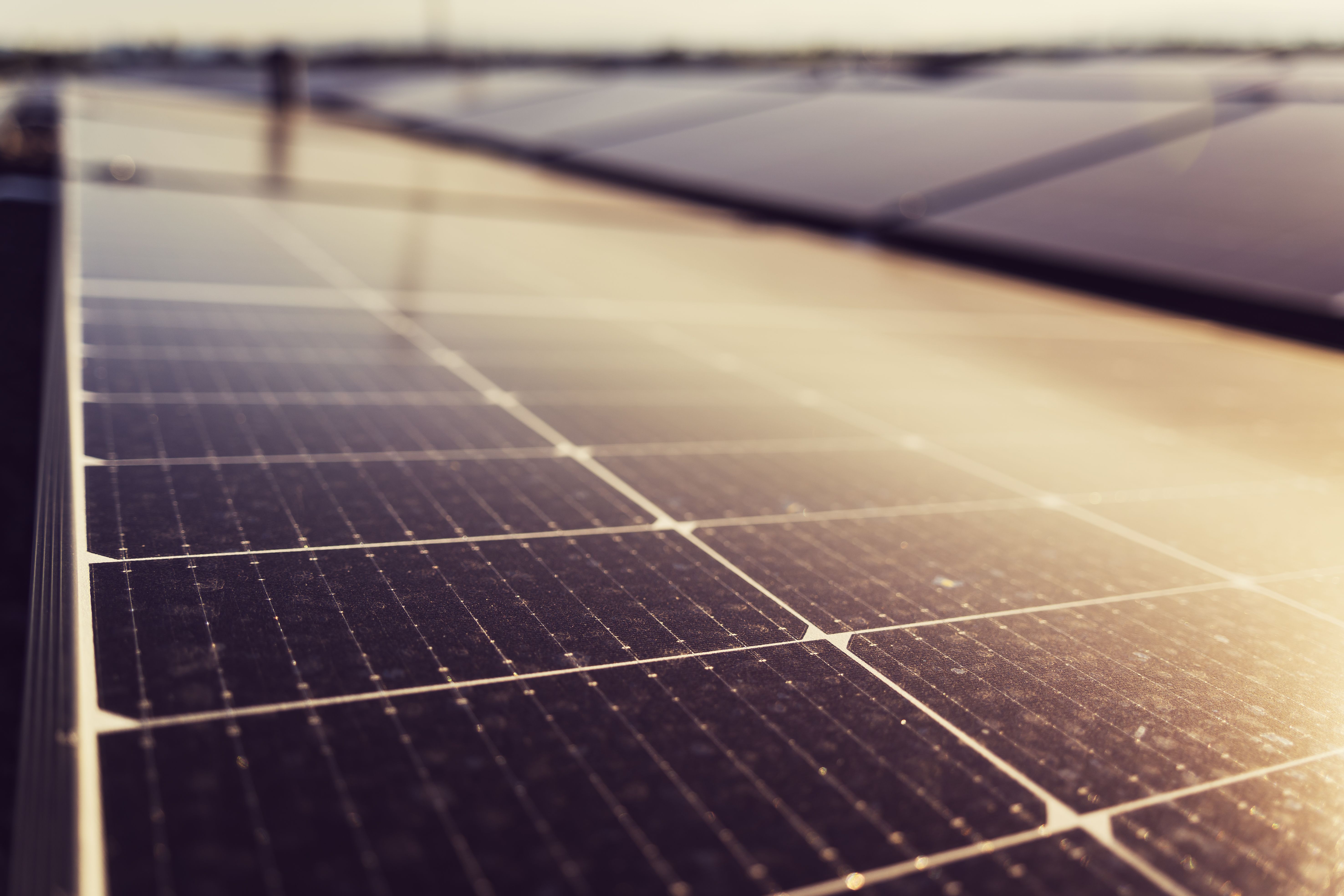


Perovskite-silicon tandem solar cells have become the clearest path to a real jump in solar-panel efficiency in decades, and their patent landscape is distinctive because the underlying physics gives every developer the same target while leaving wide latitude in how to reach it. A single-junction silicon cell is capped by a physical ceiling that combines the Shockley-Queisser detailed-balance limit with Auger recombination losses; a Fraunhofer ISE analysis that combines both effects puts the accurate theoretical efficiency limit for a silicon-based monolithic tandem at 43.2 percent¹. The path to that ceiling runs through several distinct patenting layers. Interface passivation is currently the dominant lever on record efficiency: mixed self-assembled monolayer (SAM) contacts first enabled a certified 28.3 percent tandem², further interface-passivation work pushed a certified cell to 31.25 percent³, and subsequent bilayer SAM strategies have continued to close the non-radiative recombination gap⁴. A separate, equally central problem is depositing perovskite uniformly onto the pyramid-textured surface of industrial silicon wafers — the texture that gives production-grade silicon its light-trapping advantage also makes uniform, defect-free perovskite deposition difficult, typically causing localized electrical leakage at the pyramid peaks. Proposed fixes include selective passivation of the pyramid tips specifically (32.9 percent reported)⁵, "iceberg-like" pyramid engineering compatible with industrial texturing (33 percent)⁶, and advanced light-management approaches for textured interfaces more broadly⁷. Because record efficiency and manufacturable durability are driven by different, not always overlapping, sets of techniques, freedom-to-operate and white space analysis must span composition, interface, and texture-compatible process together.
The field has moved from a laboratory curiosity to early commercial shipment within the past two years, even as the record-chasing and the product-shipping efforts remain distinct. The current widely cited two-terminal cell efficiency record is 34.85 percent, announced by LONGi and stated by the company to be NREL-certified — a figure that should be read as certified-per-developer disclosure at cell area, since the independent certification certificate itself was not directly available in this research pass, and it is not (as of this writing) also a peer-reviewed published result⁸. This record is categorically distinct from module-level performance: Oxford PV and Fraunhofer ISE reported a full-size commercial-format module at 25 percent efficiency, a genuinely different, lower, and non-comparable figure because module-area results inherently lag cell-area records⁹. Preserving this cell-versus-module distinction, and the related single-junction-perovskite-versus-tandem distinction, matters throughout any reading of the field's efficiency claims. Commercial shipment and pilot-line status is confirmed via primary company disclosure for Oxford PV⁹; comparable primary shipment-volume disclosures for other major developers were not located in this pass and should be treated as unconfirmed pending each company's own investor-relations or regulatory filing. Because applications publish about eighteen months after filing, the most recent passivation and encapsulation filings are under-represented, so the current frontier is more active than granted-patent counts suggest.
The strategic picture turns on which side of the record-versus-durability divide an owner is defending. Efficiency-record IP, concentrated in interface-passivation chemistry, is advancing quickly through a small number of well-resourced developers and research groups, and durability improvements are increasingly bundled with efficiency claims rather than reported separately in the most recent literature. The more open, commercially decisive ground remains the manufacturing and durability layer: deposition techniques compatible with textured industrial silicon at scale, and encapsulation and barrier-layer chemistry that closes the stability gap with silicon's multi-decade outdoor lifetime. Reading the landscape by layer, technique, and owner, and tracking both the patents and the underlying materials-science research, is what separates a workable manufacturing position from a blocked one.
Where the perovskite-silicon tandem white space is
Textured-silicon-compatible deposition. Depositing a uniform, leakage-free perovskite layer onto the pyramid-textured surface of industrial silicon wafers, rather than the flat substrates used for the highest record cells, is the central manufacturing barrier standing between lab records and mass production, with several distinct proposed solutions still competing⁵,⁶,⁷.
Encapsulation and durability chemistry bundled with efficiency. The most recent passivation literature increasingly targets stability and efficiency together rather than treating them as separate problems, which is itself a signal of where the field is converging.
Verified, primary-sourced commercial shipment data. Commercial shipment status is confirmed for Oxford PV via primary disclosure; comparable confirmation for other major developers remains outstanding, making rigorously verified shipment and production-volume claims a genuine differentiator.
Module-scale (not just cell-scale) efficiency. Because record efficiency is consistently reported at small cell area while commercial products are judged at full module scale, IP and technique that closes this cell-to-module gap is disproportionately valuable relative to further small-area record chasing.
Flexible and building-integrated form factors. Solution-processable, flexible tandem cells for curved surfaces, windows, and other building-integrated applications exploit perovskite's inherent advantages rather than competing directly with rigid silicon, and remain a less-crowded adjacent frontier.
How AI-powered landscape and white space analysis helps
Resolving a landscape that spans perovskite composition, interface chemistry, texture-compatible deposition, and encapsulation — where record-setting efficiency claims are announced by multiple developers within the same quarter, and where cell-area, module-area, certified, and company-announced figures are easily conflated — requires more than keyword search. AI-powered analysis addresses this with semantic search that clusters activity by layer and technique across varied terminology, attribution that normalizes solar-manufacturer, materials-supplier, and research-institution filers to canonical entities, and continuous monitoring that keeps pace with a field where the efficiency record itself changes multiple times a year. Because photovoltaics advances appear in materials-science literature before they are patented, reading both patents and literature gives the earliest signal of which technique is actually closing the gap between record cell and bankable product.
The competitive landscape by the numbers
The perovskite/tandem solar-cell patent family set totals roughly 12,575 documents, though this figure includes broader "tandem solar cell" and general photovoltaics art and therefore overstates perovskite-silicon-specific filings on its own (Cypris corpus, indicative; 2025–26 partial). Geography is led by China (approximately 1,994 families) and the United States (approximately 1,623), followed by Germany (approximately 846), Japan (approximately 773), and South Korea (approximately 758) (Cypris corpus, indicative; 2025–26 partial). Top assignees mix photovoltaics incumbents and materials firms — Trina Solar, Oxford Photovoltaics, Kaneka, LG, BASF, CEA, and JinkoSolar — alongside broader electronics players such as Canon and Toshiba, whose filings contribute some non-perovskite tandem/PV art to the set (Cypris corpus, indicative; 2025–26 partial). Filings show a recent perovskite-driven resurgence, rising from roughly 526 families in 2021 to about 1,191 in 2025 (Cypris corpus, indicative; 2025–26 partial).
Where Cypris fits
Cypris runs patent landscape and white space analysis for fast-moving materials fields such as perovskite-silicon tandem photovoltaics across a corpus of more than 500 million patents and scientific papers, organized through a proprietary R&D ontology. The ontology clusters activity by layer, perovskite composition, interface passivation, tandem architecture, and encapsulation, and normalizes solar-manufacturer, materials-supplier, and research-institution filers to canonical entities, so a team can resolve which layers and techniques are crowded and which remain open as white space. Semantic search across patents and scientific literature connects filings to the underlying materials-science research, which is where tandem-cell advances appear first, often well ahead of the patent record. Cypris Q, the platform's agentic layer, lets teams run landscape and white space analysis conversationally and chain the clustering, attribution, and gap analysis, and Agentic Monitoring tracks a defined layer over time and flags new patents and papers as they publish. Cypris provides enterprise API partnerships with OpenAI, Anthropic, and Google, and is built with enterprise-grade security. Cypris serves hundreds of enterprise customers across pharmaceuticals, chemicals, advanced materials, energy, and other regulated industries.
FAQ
What is a perovskite-silicon tandem solar cell? A perovskite-silicon tandem solar cell stacks a perovskite top cell on top of a crystalline-silicon bottom cell so the combined device captures more of the solar spectrum than either material could alone, allowing it to exceed the theoretical ceiling that limits any single-junction silicon cell. That combined ceiling, accounting for both Shockley-Queisser and Auger effects, is calculated at 43.2 percent¹. The current company-reported, NREL-certified cell-area record stands at 34.85 percent⁸.
Why can't a single-junction silicon cell just be made more efficient instead? A single-junction silicon cell cannot exceed its combined Shockley-Queisser/Auger efficiency ceiling because that limit is set by the fundamental physics of extracting energy from a broad-spectrum light source using a single semiconductor bandgap, not by manufacturing quality¹. Continuing to refine single-junction silicon can approach that limit but never exceed it. Stacking a second, complementary-bandgap material is the only way to break through it.
What layers does the tandem patent landscape cover? The landscape covers perovskite composition and bandgap engineering, interface passivation chemistry, tandem cell architecture compatible with industrial silicon texturing, and encapsulation and stability engineering. Interface passivation is currently the dominant lever on record efficiency²,³,⁴, while texture-compatible deposition remains the central manufacturing barrier⁵,⁶,⁷. A bankable product depends on progress across all of these layers together.
Are perovskite-silicon tandem panels available to buy in 2026? Only in limited volume, and only confirmed for certain developers. Oxford PV has a confirmed primary disclosure of a full-size commercial-format module reaching 25 percent efficiency in partnership with Fraunhofer ISE⁹, but comparable shipment-volume confirmation for other major manufacturers was not available in current primary disclosures. The efficiency record (34.85 percent, cell-area) and the shipping product (25 percent, module-area) are currently very different numbers describing different things.
Where is the white space in perovskite-silicon tandem solar cells? The white space includes textured-silicon-compatible deposition, durability chemistry bundled with efficiency gains, verified commercial shipment data, closing the cell-to-module efficiency gap, and flexible or building-integrated form factors. Record-efficiency IP is advancing quickly through interface-passivation chemistry specifically. The manufacturing, durability, and module-scale layers are the more open and commercially decisive ground.
Why is depositing perovskite onto textured silicon so hard? Depositing perovskite onto textured silicon is hard because industrial silicon wafers use a pyramid-textured surface to trap light and boost efficiency, but that same texture makes it difficult to deposit a uniform, defect-free perovskite layer, often causing localized electrical leakage at the pyramid peaks. The highest record cells are typically demonstrated on flatter or smaller-area substrates that partially avoid this problem. Multiple distinct fixes are being pursued in parallel, including selective peak passivation and engineered pyramid geometry⁵,⁶.
Why does perovskite-silicon tandem analysis need scientific literature? Perovskite-silicon tandem analysis needs scientific literature because composition, passivation, and encapsulation advances appear in materials-science research before they are patented, and because distinguishing certified from company-announced figures, and cell-area from module-area results, requires reading the primary literature rather than press coverage. Analyzing patents alone gives a lagging view. Cypris analyzes both across more than 500 million patents and scientific papers.
Which teams use perovskite-silicon tandem patent landscape analysis? Perovskite-silicon tandem patent landscape analysis is used by R&D, IP, and strategy teams at solar manufacturers and materials suppliers, as well as investors assessing the photovoltaics sector. Because record efficiency and commercial durability are driven by different techniques at different maturity levels, and because efficiency claims require careful certified-versus-announced and cell-versus-module verification, structured analysis is essential. Cypris serves hundreds of enterprise customers across advanced materials, energy, and other research-intensive industries.
Endnotes
- Schubert MC, Glunz SW, Fell A, Bivour M, Messmer C. Elucidating the efficiency limit of silicon-based monolithic tandem cells through the combination of Auger and Shockley-Queisser limits. EES Solar. DOI: 10.1039/d5el00085h.
- Kishimoto K, Uzu H, Yamamoto K, Yoshida W, Okamoto S. 28.3% efficient perovskite-silicon tandem solar cells with mixed self-assembled monolayers. Applied Physics Express. DOI: 10.35848/1882-0786/ac727b.
- Artuk K, Sahli F, Jeangros Q, Boccard M, Tabean S. Interface passivation for 31.25%-efficient perovskite/silicon tandem solar cells. Science. DOI: 10.1126/science.adg0091.
- Jia Y, Xu X, Li P, Li Z, Xiao C. Perovskite/silicon tandem solar cells with bilayer interface passivation. Nature. DOI: 10.1038/s41586-024-07997-7.
- Ye JP, Yang X, Ying Z, Du H, Yang W. Selective passivation of pyramid peaks for 32.9%-efficient perovskite/silicon tandem solar cells. Matter. DOI: 10.1016/j.matt.2026.102824.
- Wei J, Li R, Yu X, Hang P, Wu T. Iceberg-like pyramids in industrially textured silicon enabled 33% efficient perovskite-silicon tandem solar cells. Nature Communications. DOI: 10.1038/s41467-025-62389-3.
- Stannowski B, Korte L, Jošt M, Al-Ashouri A, Lipovšek B. Textured interfaces in monolithic perovskite/silicon tandem solar cells: advanced light management for improved efficiency and energy yield. Energy & Environmental Science. DOI: 10.1039/c8ee02469c.
- LONGi Green Energy. 34.85%! LONGi Breaks World Record for Crystalline Silicon-Perovskite Tandem Solar Cell Efficiency Again. Company press release, longi.com.
- Oxford PV and Fraunhofer ISE. Oxford PV and Fraunhofer ISE Develop Full-sized Tandem PV Module with Record Efficiency of 25 Percent. Fraunhofer ISE press release, ise.fraunhofer.de.
- Cypris platform corpus analysis, perovskite/tandem solar-cell patent families. Indicative figures; 2025–2026 partial.